- 您现在的位置:买卖IC网 > Sheet目录3855 > PIC16C62B-20/SS (Microchip Technology)IC MCU OTP 2KX14 PWM 28SSOP
PIC16C62B/72A
DS35008B-page 8
Preliminary
1999 Microchip Technology Inc.
2.2
Data Memory Organization
The data memory is partitioned into multiple banks
which contain the General Purpose Registers and the
Special Function Registers. Bits RP1 and RP0 are the
bank select bits.
= 00
→ Bank0
= 01
→ Bank1
= 10
→ Bank2 (not implemented)
= 11
→ Bank3 (not implemented)
Each bank extends up to 7Fh (128 bytes). The lower
locations of each bank are reserved for the Special
Function Registers. Above the Special Function Regis-
ters are General Purpose Registers, implemented as
static RAM. All implemented banks contain Special
Function Registers. Some “high use” Special Function
Registers from one bank may be mirrored in another
bank for code reduction and quicker access.
2.2.1
GENERAL PURPOSE REGISTER FILE
The register file can be accessed either directly, or indi-
rectly
through
the
File
Select
Register
FSR
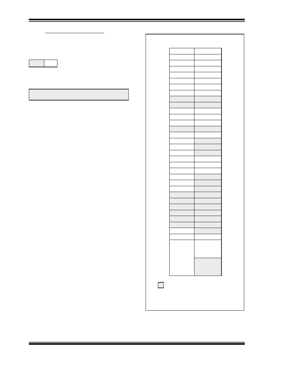
FIGURE 2-2:
REGISTER FILE MAP
RP1(1)
RP0
(STATUS<6:5>)
Note 1: Maintain this bit clear to ensure upward compati-
bility with future products.
Unimplemented data memory locations,
read as ’0’.
Note 1: Not a physical register.
2:
These registers are not implemented on the
PIC16C62B, read as ’0’.
File
Address
File
Address
00h
INDF(1)
80h
01h
TMR0
OPTION_REG 81h
02h
PCL
82h
03h
STATUS
83h
04h
FSR
84h
05h
PORTA
TRISA
85h
06h
PORTB
TRISB
86h
07h
PORTC
TRISC
87h
08h
—
88h
09h
—
89h
0Ah
PCLATH
8Ah
0Bh
INTCON
8Bh
0Ch
PIR1
PIE1
8Ch
0Dh
—
8Dh
0Eh
TMR1L
PCON
8Eh
0Fh
TMR1H
—
8Fh
10h
T1CON
—
90h
11h
TMR2
—
91h
12h
T2CON
PR2
92h
13h
SSPBUF
SSPADD
93h
14h
SSPCON
SSPSTAT
94h
15h
CCPR1L
—
95h
16h
CCPR1H
—
96h
17h
CCP1CON
—
97h
18h
—
98h
19h
—
99h
1Ah
—
9Ah
1Bh
—
9Bh
1Ch
—
9Ch
1Dh
—
9Dh
1Eh
ADRES(2)
—
9Eh
1Fh
ADCON0(2)
ADCON1(2)
9Fh
20h
General
Purpose
Registers
General
Purpose
Registers
A0h
BFh
—
C0h
—
7Fh
—
FFh
Bank 0
Bank 1
发布紧急采购,3分钟左右您将得到回复。
相关PDF资料
PIC16LC711-04I/SO
IC MCU OTP 1KX14 A/D 18SOIC
PIC18F66J90-I/PT
IC PIC MCU FLASH 64KB 64-TQFP
ATMEGA32L-8AC
IC AVR MCU 32K LV 8MHZ COM44TQFP
DSPIC30F2012-30I/SP
IC DSPIC MCU/DSP 12K 28DIP
PIC18LF2321-I/ML
IC PIC MCU FLASH 4KX16 28QFN
PIC18F4321-I/P
IC PIC MCU FLASH 4KX16 40DIP
ATMEGA32L-8MC
IC AVR MCU 32K LV 8MHZ COM 44QFN
PIC18F2450-I/SP
IC PIC MCU FLASH 8KX16 28DIP
相关代理商/技术参数
PIC16C62B-20E/SO
功能描述:8位微控制器 -MCU 3.5KB 128 RAM 22 I/O RoHS:否 制造商:Silicon Labs 核心:8051 处理器系列:C8051F39x 数据总线宽度:8 bit 最大时钟频率:50 MHz 程序存储器大小:16 KB 数据 RAM 大小:1 KB 片上 ADC:Yes 工作电源电压:1.8 V to 3.6 V 工作温度范围:- 40 C to + 105 C 封装 / 箱体:QFN-20 安装风格:SMD/SMT
PIC16C62B-20E/SP
功能描述:8位微控制器 -MCU 3.5KB 128 RAM 22 I/O RoHS:否 制造商:Silicon Labs 核心:8051 处理器系列:C8051F39x 数据总线宽度:8 bit 最大时钟频率:50 MHz 程序存储器大小:16 KB 数据 RAM 大小:1 KB 片上 ADC:Yes 工作电源电压:1.8 V to 3.6 V 工作温度范围:- 40 C to + 105 C 封装 / 箱体:QFN-20 安装风格:SMD/SMT
PIC16C62B-20E/SS
功能描述:8位微控制器 -MCU 3.5KB 128 RAM 22 I/O RoHS:否 制造商:Silicon Labs 核心:8051 处理器系列:C8051F39x 数据总线宽度:8 bit 最大时钟频率:50 MHz 程序存储器大小:16 KB 数据 RAM 大小:1 KB 片上 ADC:Yes 工作电源电压:1.8 V to 3.6 V 工作温度范围:- 40 C to + 105 C 封装 / 箱体:QFN-20 安装风格:SMD/SMT
PIC16C62B-20I/ML
功能描述:8位微控制器 -MCU 3.5KB 128 RAM 22 I/O RoHS:否 制造商:Silicon Labs 核心:8051 处理器系列:C8051F39x 数据总线宽度:8 bit 最大时钟频率:50 MHz 程序存储器大小:16 KB 数据 RAM 大小:1 KB 片上 ADC:Yes 工作电源电压:1.8 V to 3.6 V 工作温度范围:- 40 C to + 105 C 封装 / 箱体:QFN-20 安装风格:SMD/SMT
PIC16C62B-20I/SO
功能描述:8位微控制器 -MCU 3.5KB 128 RAM 22 I/O RoHS:否 制造商:Silicon Labs 核心:8051 处理器系列:C8051F39x 数据总线宽度:8 bit 最大时钟频率:50 MHz 程序存储器大小:16 KB 数据 RAM 大小:1 KB 片上 ADC:Yes 工作电源电压:1.8 V to 3.6 V 工作温度范围:- 40 C to + 105 C 封装 / 箱体:QFN-20 安装风格:SMD/SMT
PIC16C62B-20I/SO
制造商:Microchip Technology Inc 功能描述:8BIT CMOS MCU SMD 16C62 SOIC28
PIC16C62B-20I/SP
功能描述:8位微控制器 -MCU 3.5KB 128 RAM 22 I/O RoHS:否 制造商:Silicon Labs 核心:8051 处理器系列:C8051F39x 数据总线宽度:8 bit 最大时钟频率:50 MHz 程序存储器大小:16 KB 数据 RAM 大小:1 KB 片上 ADC:Yes 工作电源电压:1.8 V to 3.6 V 工作温度范围:- 40 C to + 105 C 封装 / 箱体:QFN-20 安装风格:SMD/SMT
PIC16C62B-20I/SP
制造商:Microchip Technology Inc 功能描述:IC 8BIT CMOS MCU 16C62 SDIL28